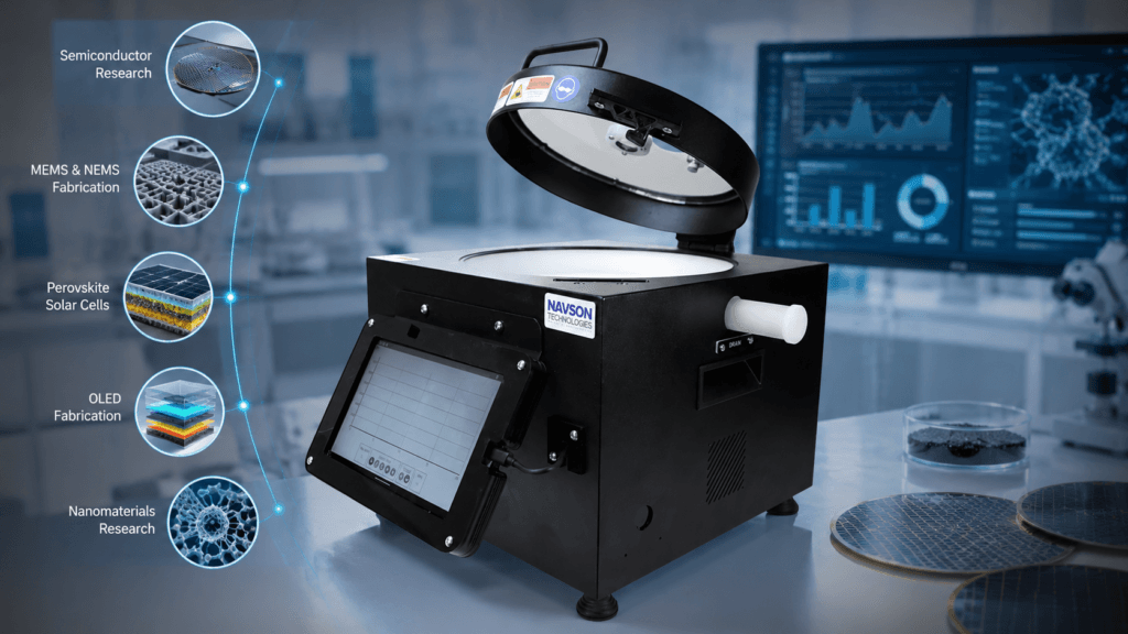
Spin Coater India
Looking for a spin coater in India for thin film deposition, photoresist coating, perovskite solar cells, OLED fabrication, MEMS devices, or nanomaterials research? Navson Technologies provides research-grade spin coating systems designed for precise thin-film deposition, process control, and scalable research workflows.
Whether you are establishing a new research laboratory, scaling semiconductor process development, or optimizing thin-film fabrication workflows, our spin coating solutions help researchers achieve consistent coating performance from early-stage experiments through advanced process development.
Download Brochures: NT12000 (6”) · NT12000 (10”) · NT10000 or Talk to an Application Engineer
Quick Answer: A spin coater is a laboratory instrument used to create highly uniform thin films on substrates through controlled rotation. In India, spin coaters are widely used in semiconductor research, photoresist lithography, perovskite solar cells, OLED development, MEMS fabrication, nanotechnology, and advanced materials research. Researchers commonly use spin coaters to create films ranging from nanometers to microns in thickness depending on solution properties, process parameters, and substrate characteristics.
Key Takeaways
- Spin coating enables controlled deposition of functional materials on flat substrates.
- Semiconductor research is one of the largest application areas.
- Glovebox-compatible systems are often required for perovskite and OLED research.
- Process repeatability is generally more important than maximum RPM.
- Advanced laboratory systems support publication-quality experimental workflows.
India’s Growing Demand for Spin Coaters
India’s semiconductor and advanced materials ecosystem is expanding rapidly, creating growing demand for spin coaters and thin-film deposition equipment. Universities, semiconductor laboratories, research institutes, and industrial R&D centers use spin coating systems for applications including photoresist lithography, MEMS fabrication, perovskite solar cells, nanomaterials, microelectronics, biosensors, and advanced battery materials. This growth is being supported by initiatives such as the India Semiconductor Mission and increased investment in domestic research and manufacturing capabilities.
Trusted by Researchers and Research Institutions
Spin coating systems are foundational process tools in semiconductor research, nanotechnology, and advanced materials development. Because coating quality directly affects device performance, researchers evaluate spin coaters based on process control, coating consistency, substrate compatibility, and long-term operational reliability.
Navson spin coating systems support universities, research institutes, semiconductor laboratories, materials science groups, and industrial R&D centers across Bengaluru, Hyderabad, Pune, Mumbai, Chennai, Ahmedabad, Kolkata, Delhi NCR, and abroad for applications including:
- Photoresist coating
- Thin film deposition
- Perovskite solar cell fabrication
- OLED research
- MEMS and NEMS device development
- Nanomaterials synthesis
- Microfluidics
- Advanced coatings research
Research Validation
Peer-reviewed publications are one of the strongest indicators of laboratory equipment performance because they demonstrate successful use in real experimental environments rather than controlled marketing demonstrations. Research using Navson spin coating systems has been published across application areas including perovskite photovoltaics, nanomaterials, thin-film electronics, photoresist processing, microfabrication, and advanced coatings — View Research Publications
Expert Insight: Many laboratories initially compare spin coaters by maximum RPM. In practice, coating uniformity, process control, substrate compatibility, acceleration profiles, and workflow requirements typically have a greater impact on research outcomes than peak rotational speed alone.
Which Spin Coater Is Right for Your Research?
Most laboratories do not need the highest-RPM spin coater. The right system depends on substrate size, coating chemistry, research workflow, glovebox requirements, and future scalability. The guide below helps identify the most suitable model based on application requirements.
Research Spin Coater Models
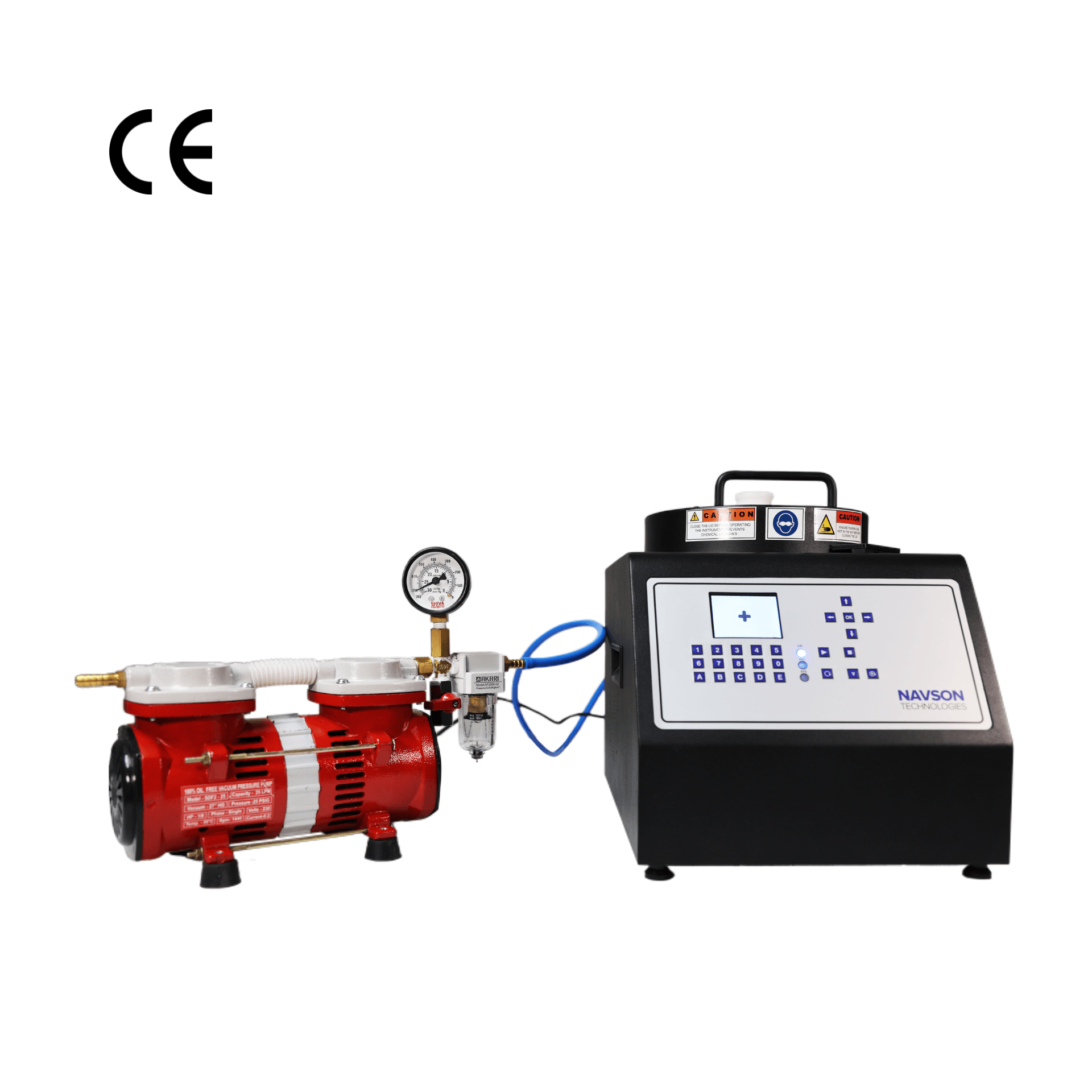
NT12000 (10″)
Designed for large substrate processing and advanced research environments,
10″ spin coating machine is ideal for:
- Substrates up to 200 mm
- Semiconductor process development
- MEMS fabrication
- Large-area thin films
- University and industrial R&D centers
Key Benefits:
- High-precision speed control
- Large substrate compatibility
- Advanced programmable recipes
- Excellent coating repeatability
View NT12000 (10″) Specifications
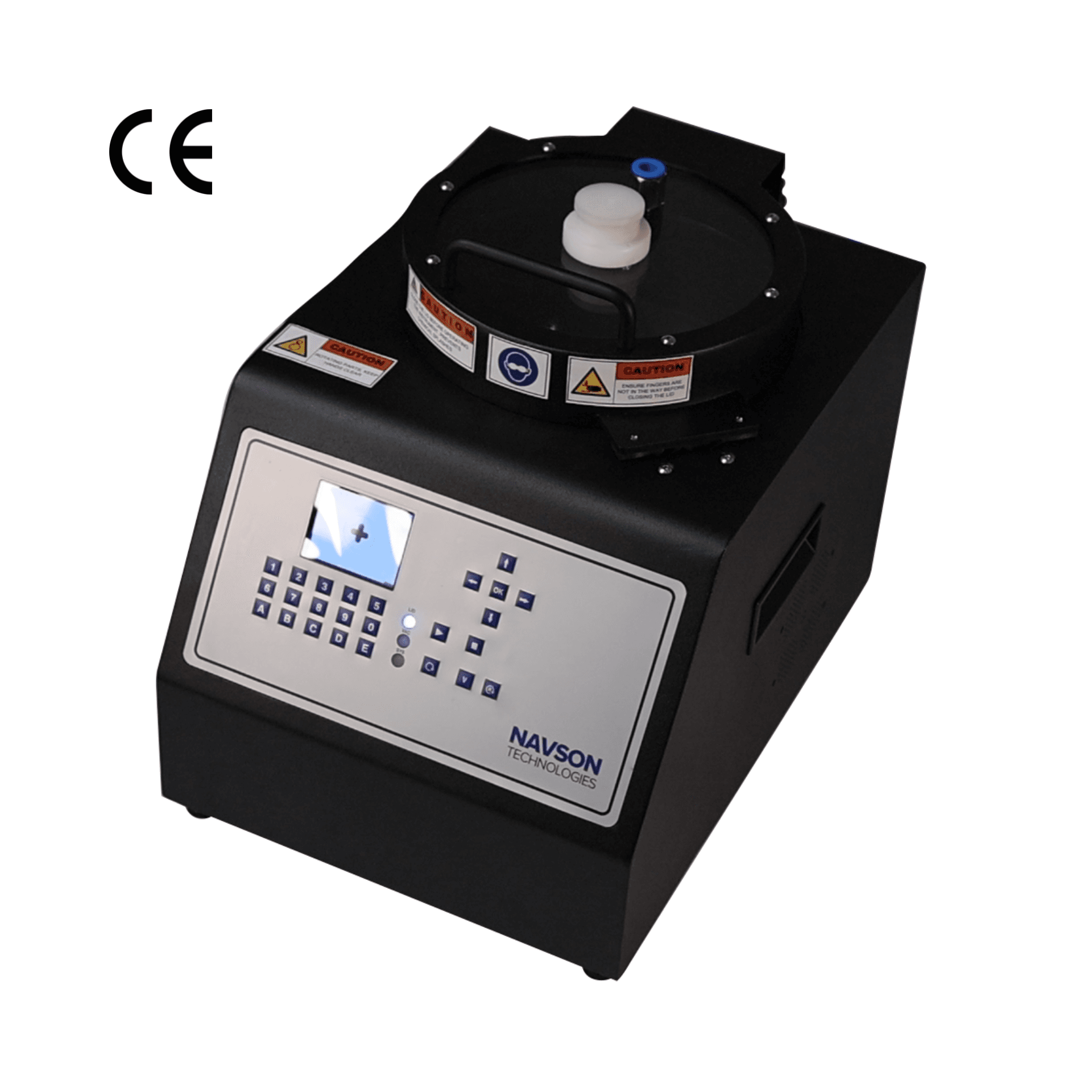
NT12000 (6″)
A compact, versatile platform optimized for modern research laboratories,
6″ Spin coating machine is ideal for:
- Substrates up to 100 mm
- Perovskite solar cells
- OLED fabrication
- Glovebox operation
- Nanomaterials research
Key Benefits:
- Compact footprint
- Glovebox compatibility
- Flexible chuck configurations
- High repeatability
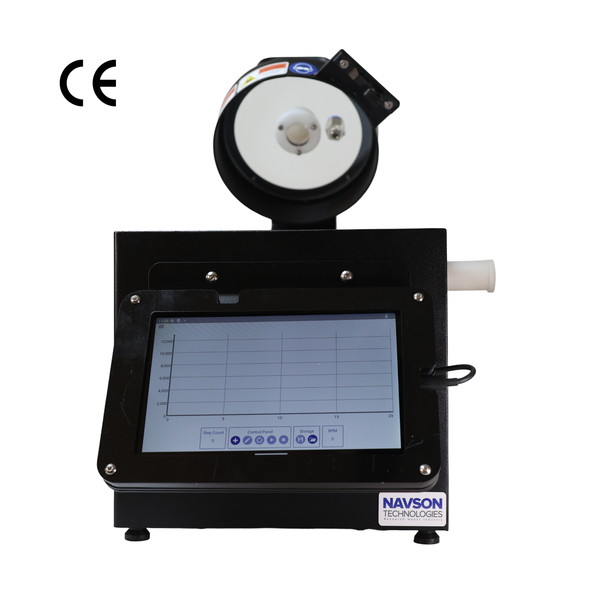
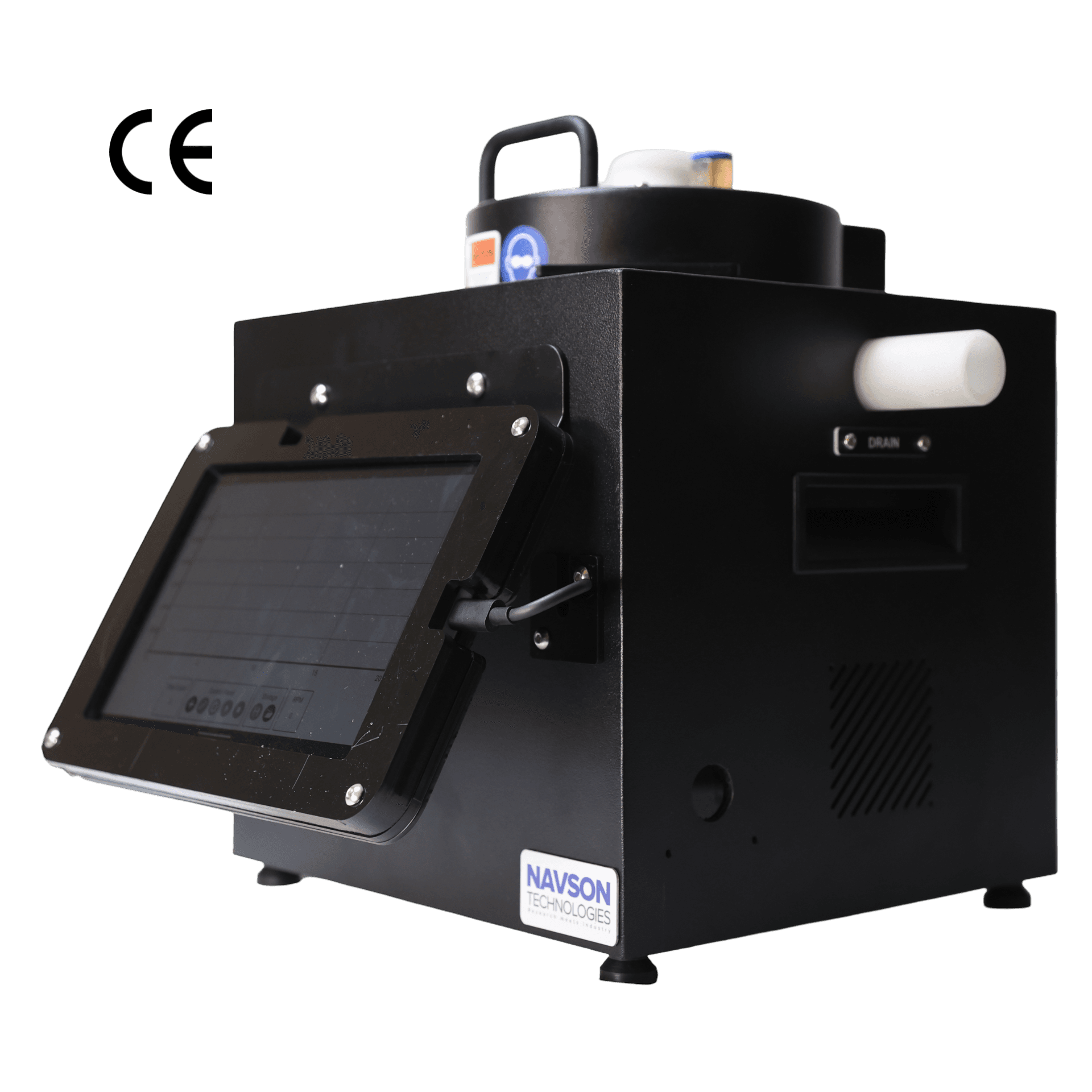
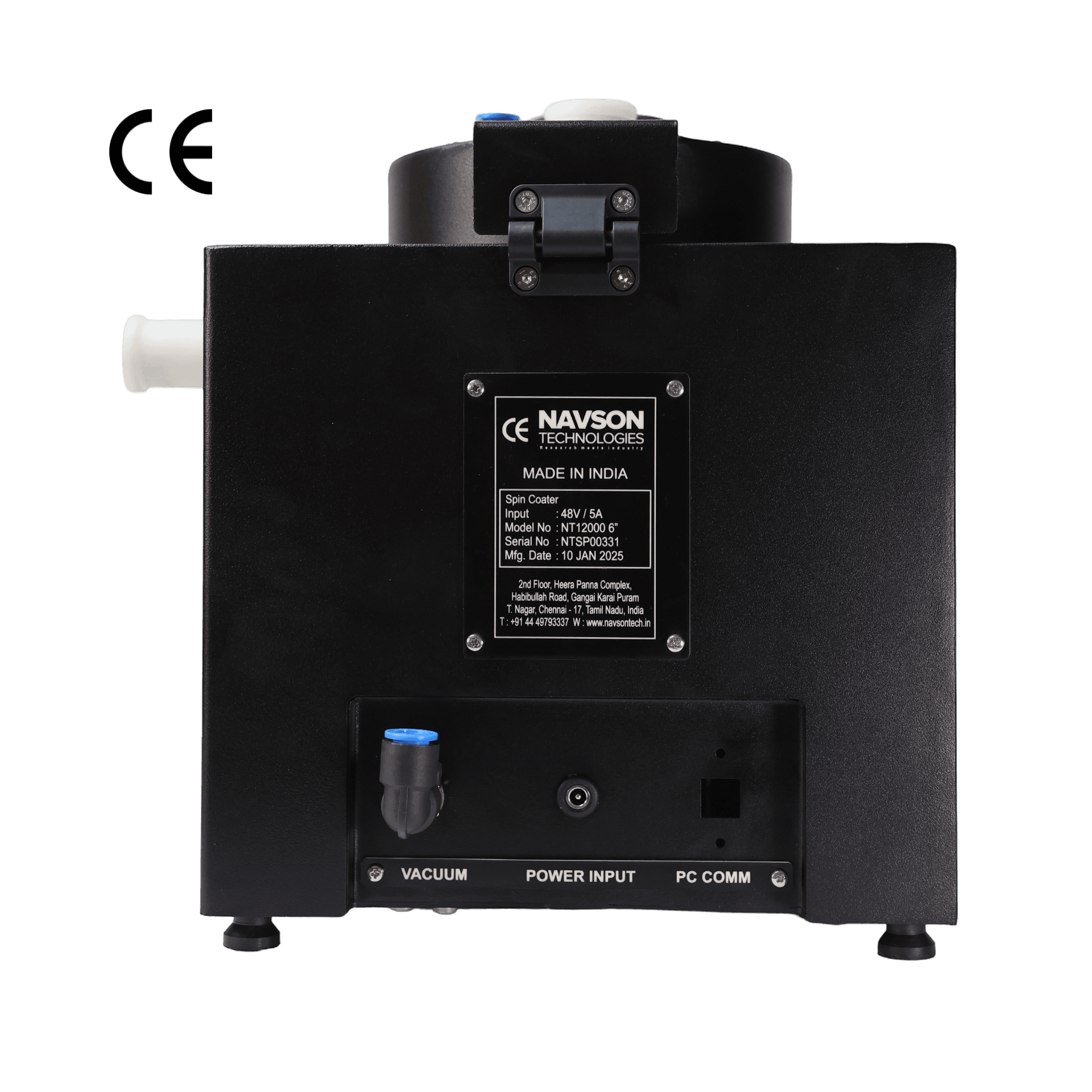
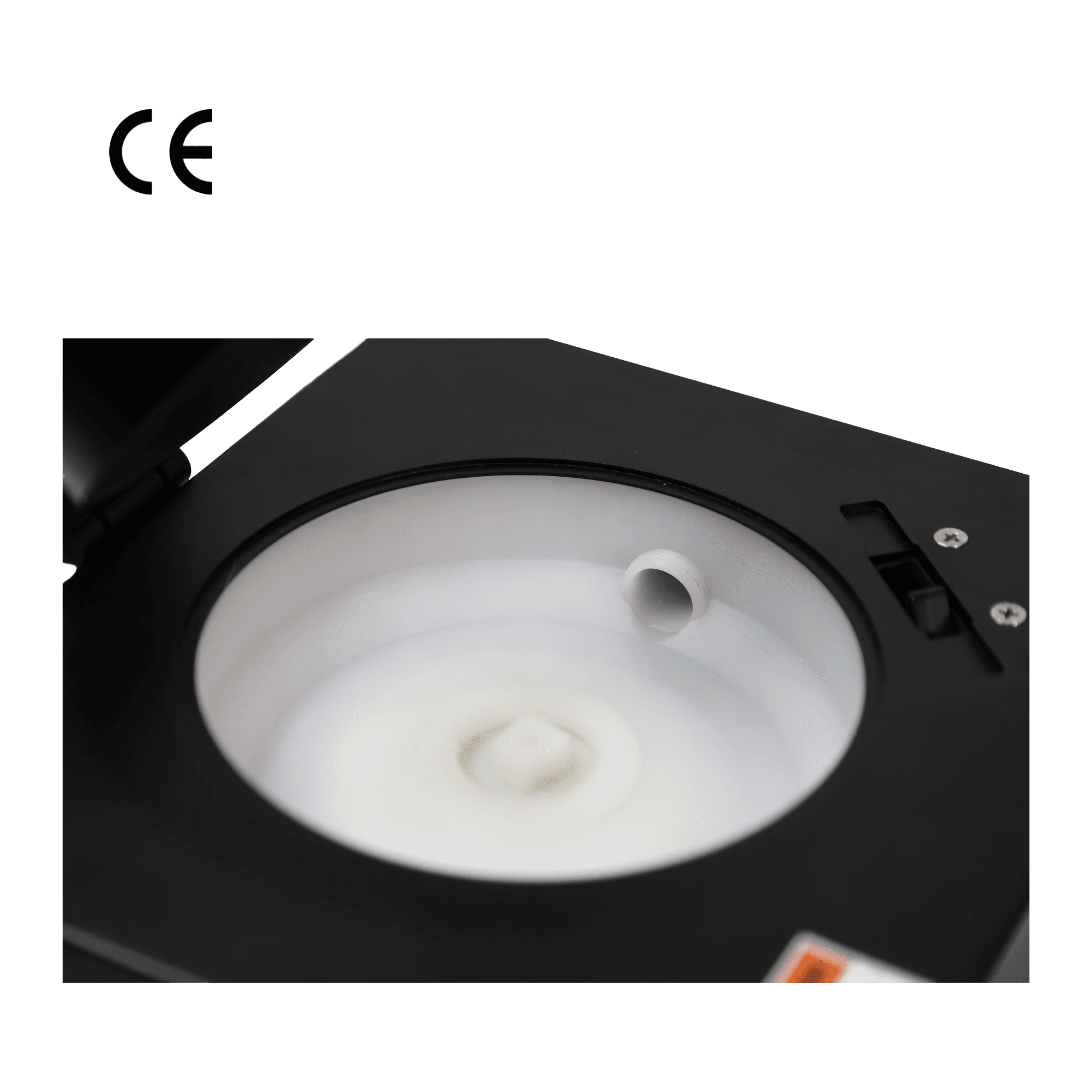
View NT12000 (6″) Specifications
NT10000
Reliable performance for general thin film and academic research applications,
This laboratory spin coater is ideal for:
- Materials science laboratories
- Academic institutions
- Research training facilities
- General thin film deposition
Key Benefits:
- User-friendly operation
- Stable RPM control
- Flexible process development
- Cost-effective research platform
How to Choose the Right Spin Coater
Selecting a spin coater depends on substrate size, research objectives, environmental requirements, and process complexity.
| Research Requirement | Recommended Model |
|---|---|
| Perovskite Solar Cells | NT12000 (6″) |
| OLED Research | NT12000 (6″) |
| Photoresist Lithography | NT12000 (10″) |
| Large Area Coatings | NT12000 (10″) |
| General Thin Film Research | NT10000 |
| Glovebox Applications | NT12000 (6″) |
| Advanced Semiconductor Research | NT12000 (10″) |
The optimal spin coater depends on substrate dimensions, coating chemistry, environmental conditions, and the level of process control required by the application. If you are unsure which system best fits your application, our application engineering team can assist with process selection and configuration recommendations.
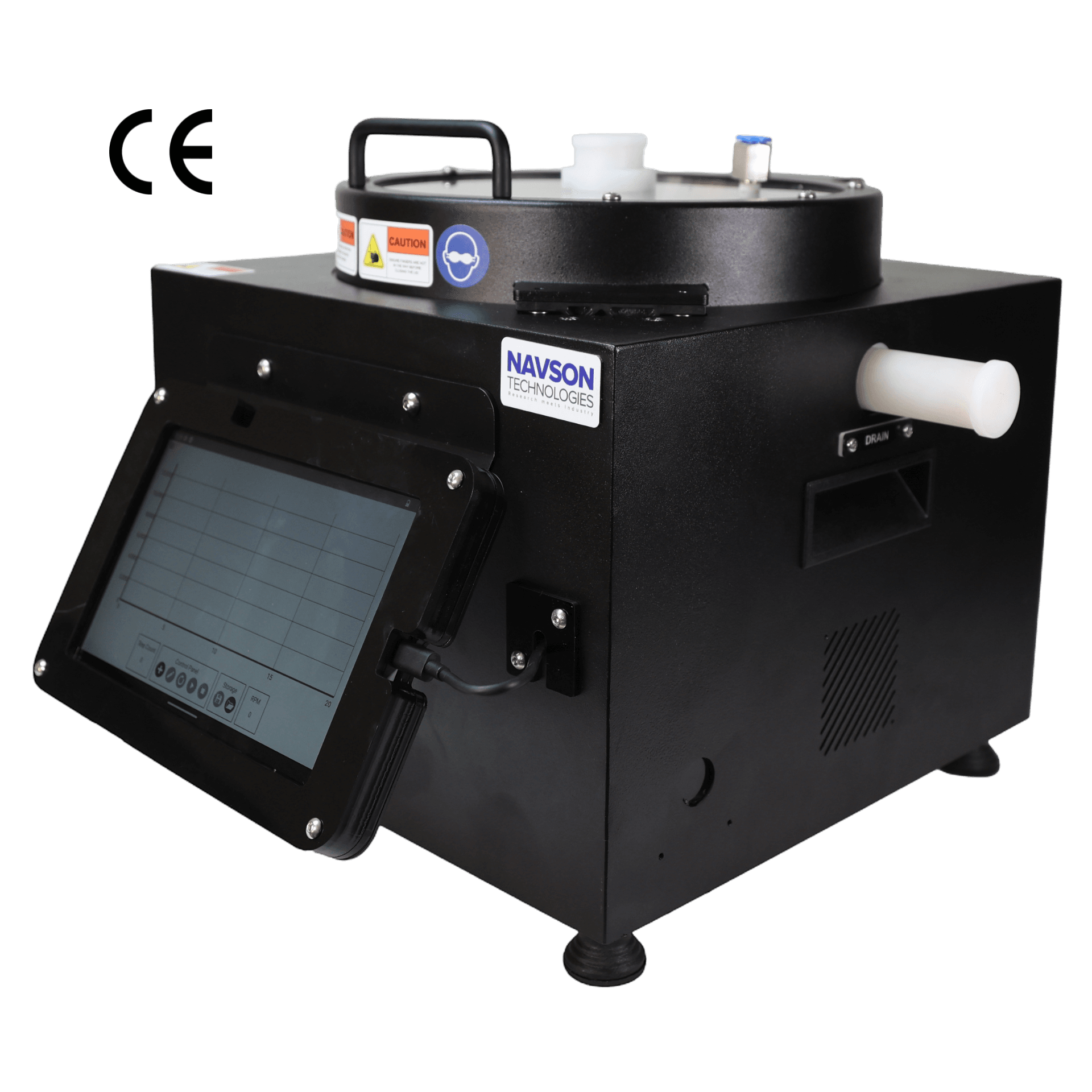
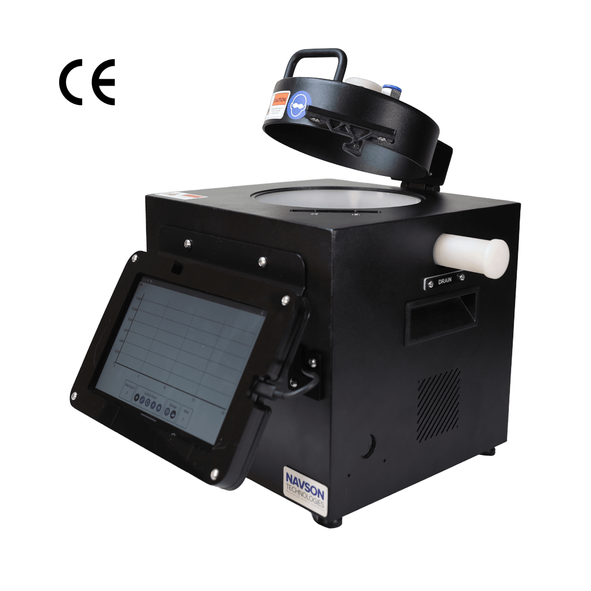
Why Researchers Choose Navson Spin Coaters
- Reproducible Thin Film Formation — Consistent process control enables repeatable film thickness and coating quality across experiments.
- Vacuum-Less Chuck Technology — Designed to simplify operation while supporting a wide range of substrates and research workflows.
- Vacuum, Vacuum-Free and Hybrid Configurations — Researchers can select the chuck architecture best suited to their materials and process requirements.
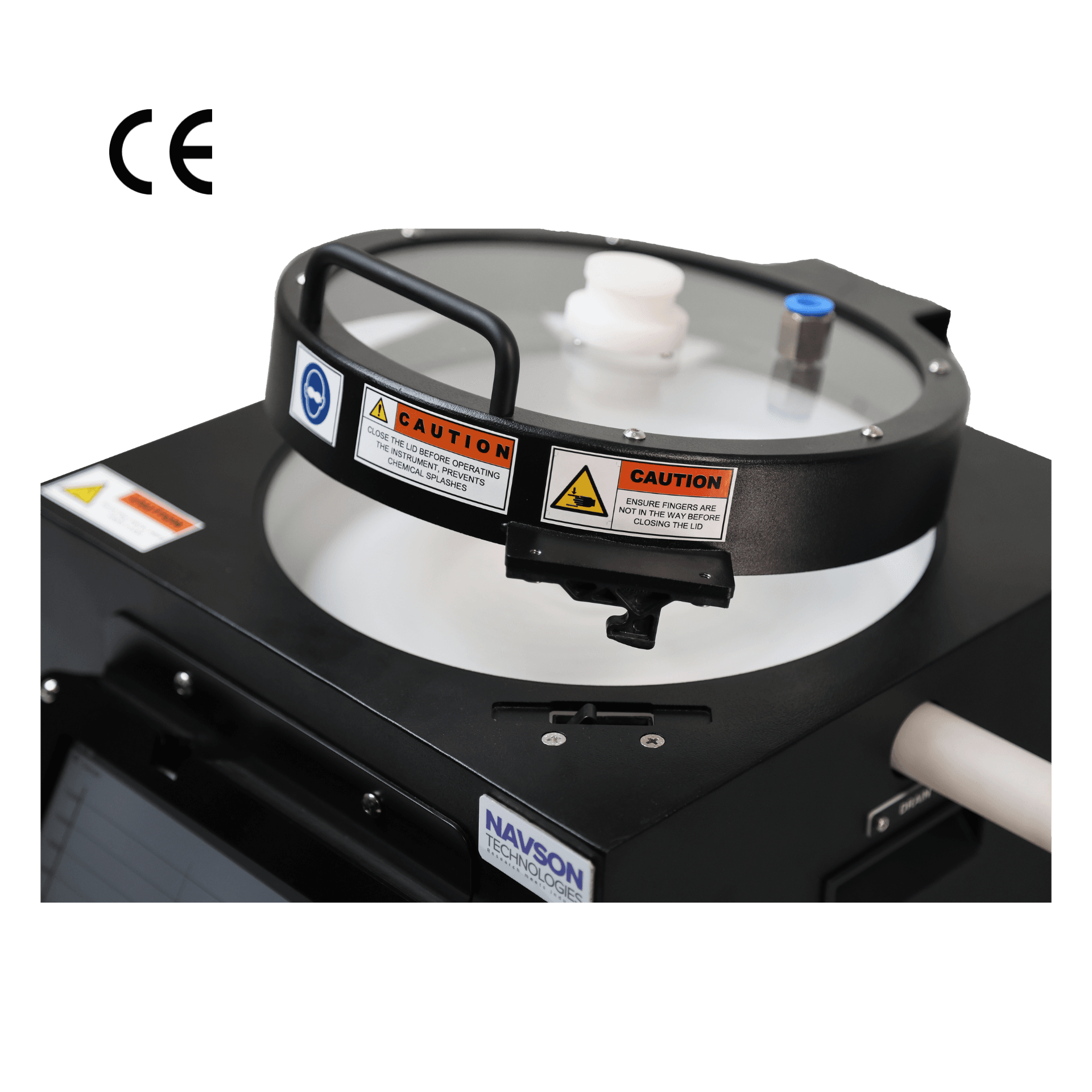
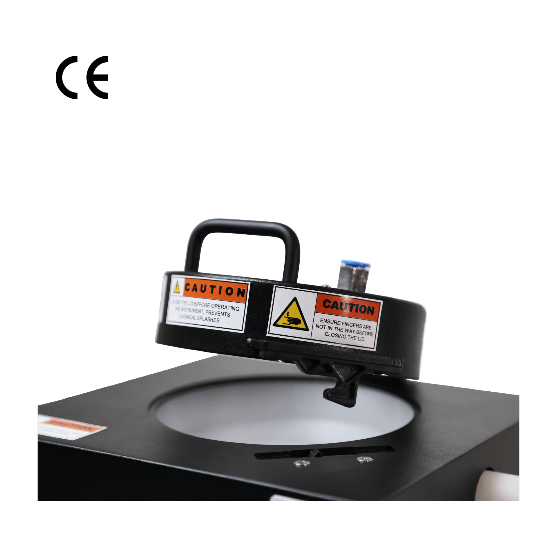
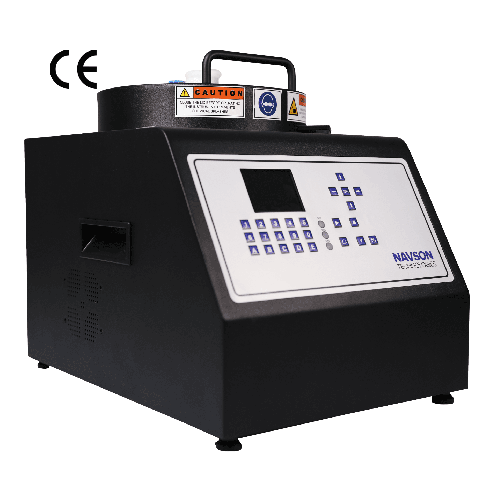
- Glovebox Compatibility — Suitable for moisture-sensitive and oxygen-sensitive materials including perovskite and advanced organic semiconductor research. Supports oxygen-sensitive and moisture-sensitive research materials.
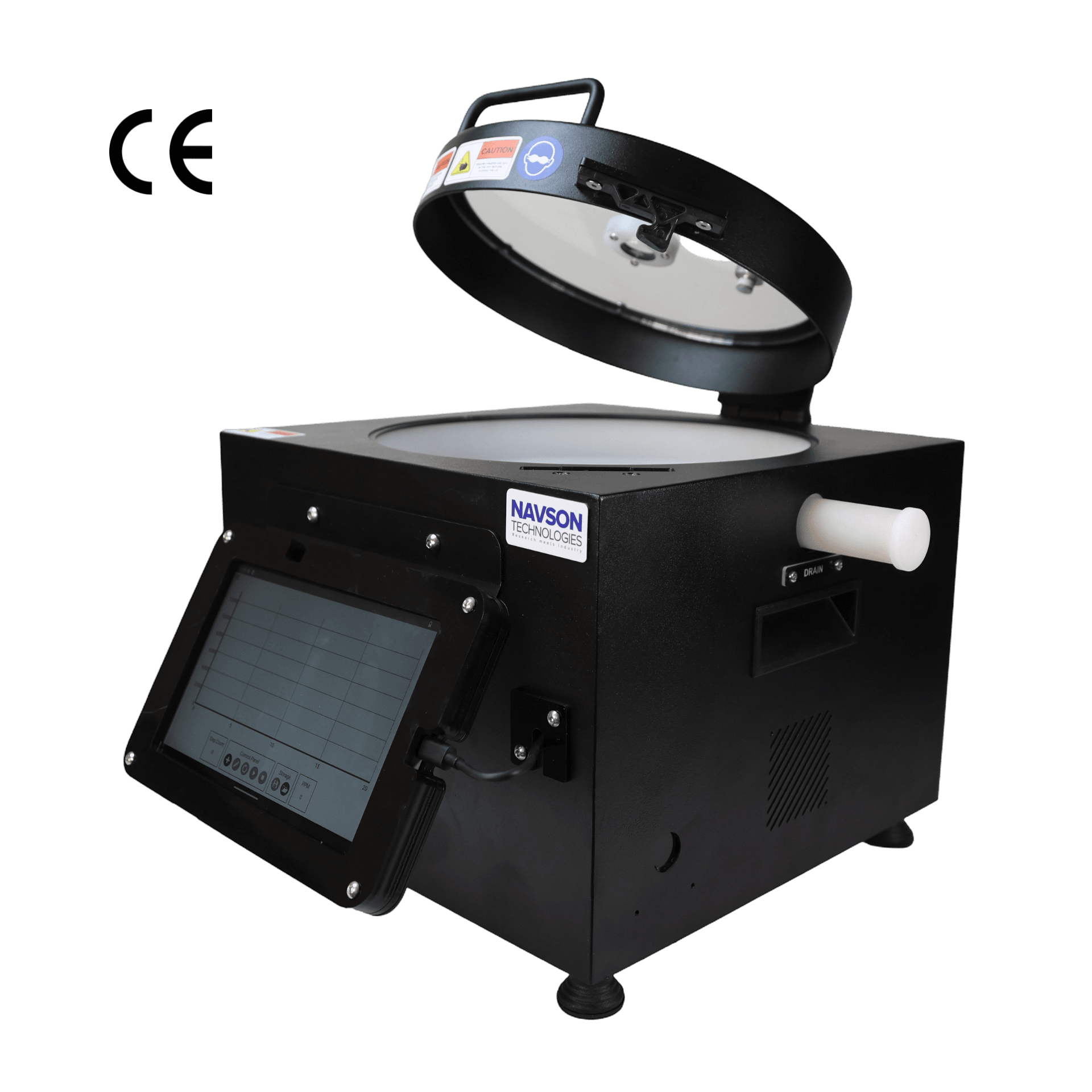
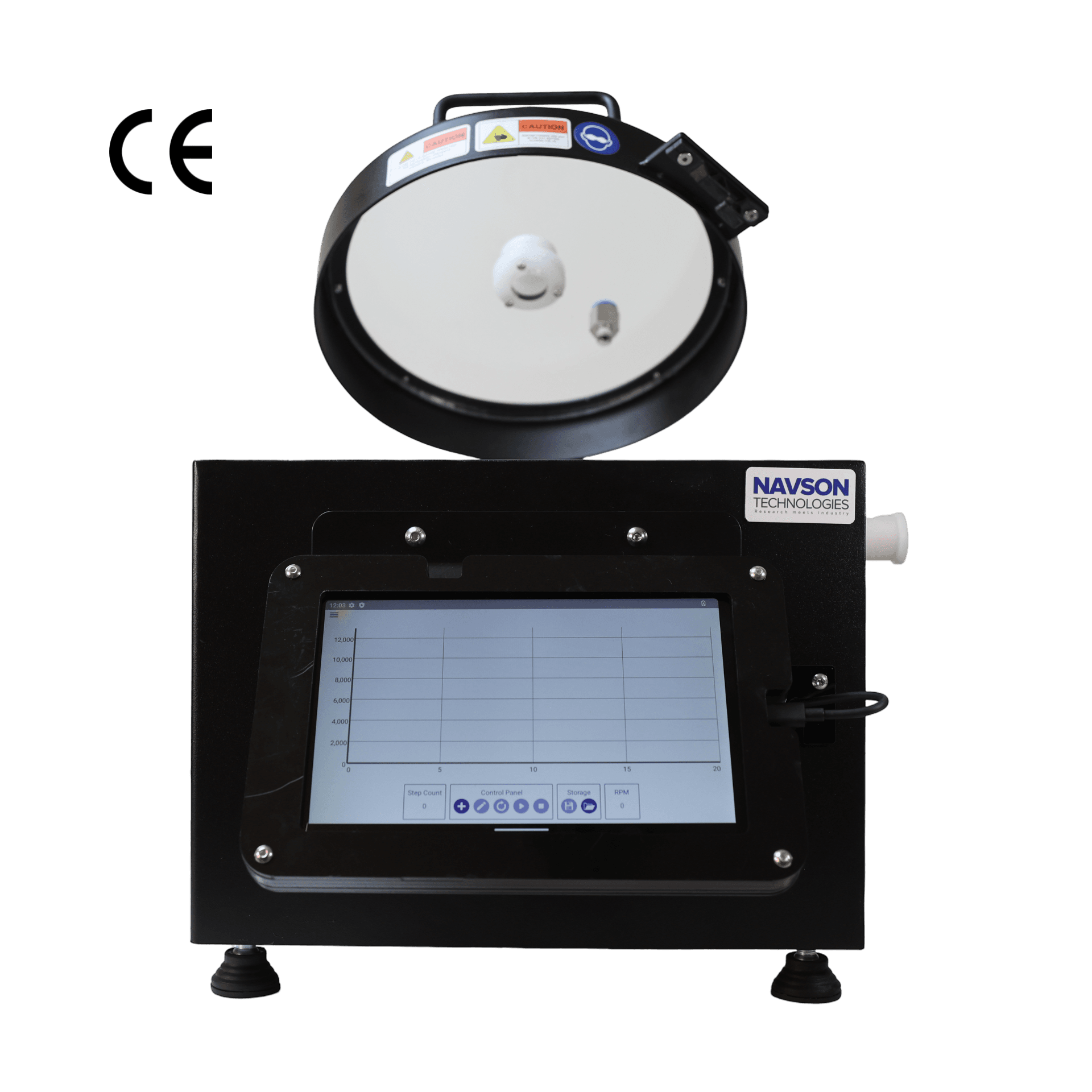
- ±1% RPM Accuracy — Precision speed control helps improve coating consistency and process repeatability. Critical for reproducible coating thickness and process validation.
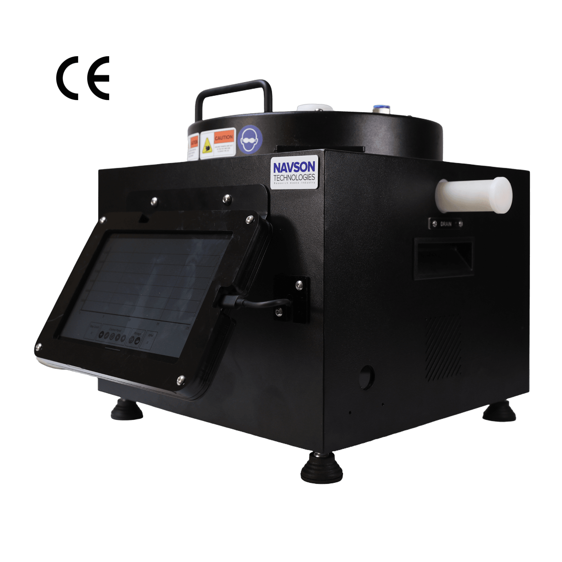
- Polypropylene Process Chamber — Designed for compatibility with a broad range of laboratory coating applications.
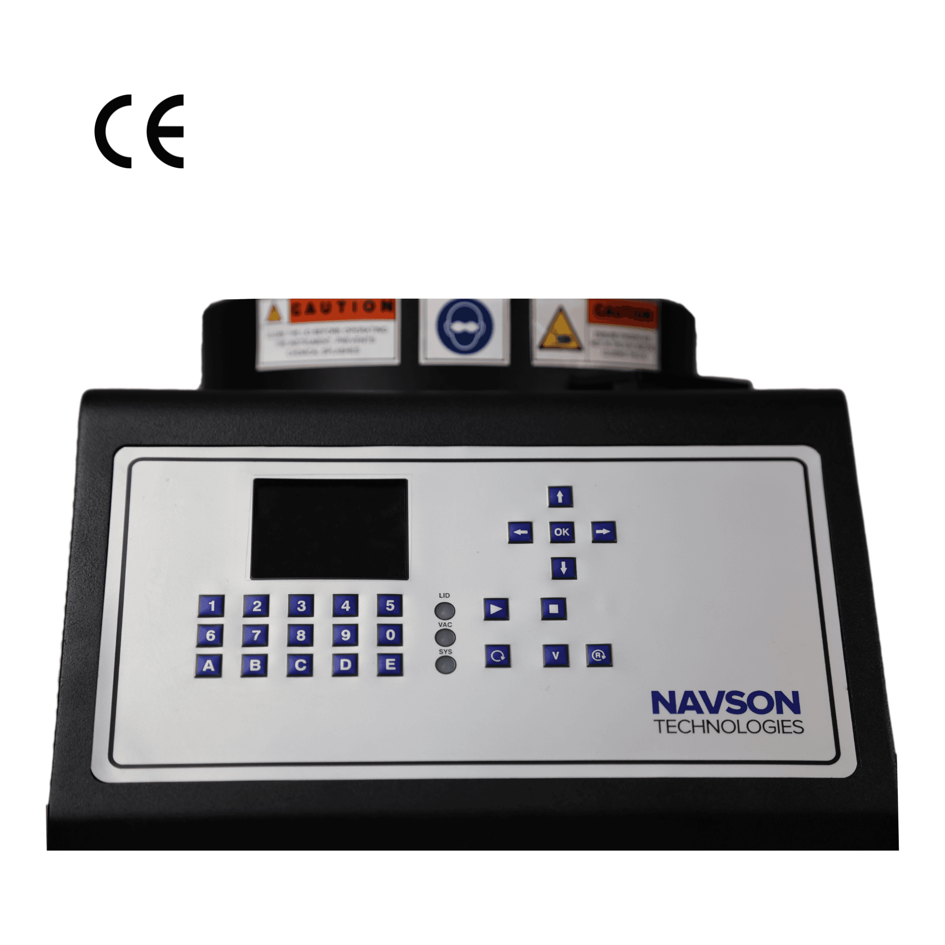
- OTA Software Updates — Continuous software enhancements help laboratories maintain modern process capabilities.
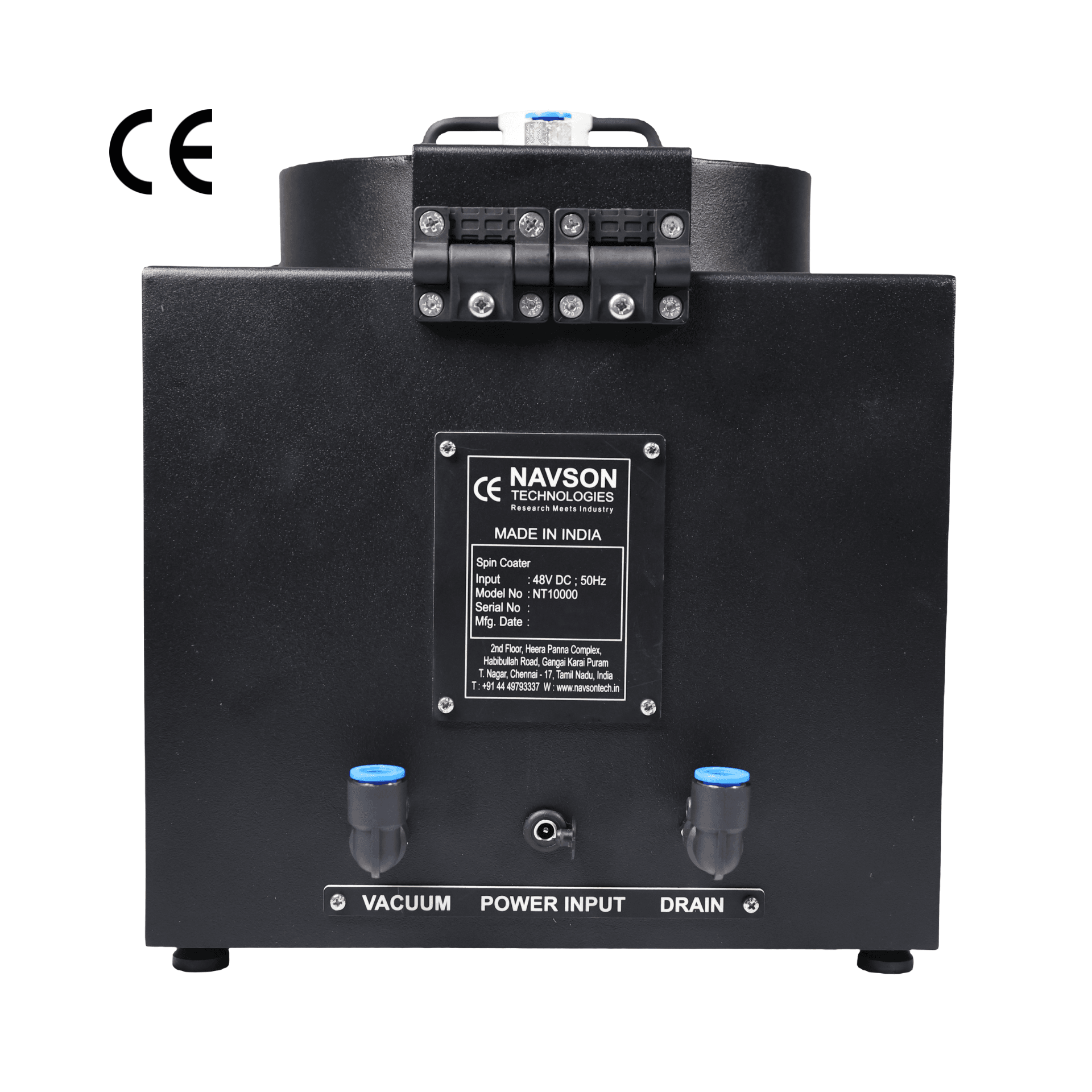
- Made in India with Local Technical Support — Faster Service Response, and Application Engineering Assistance.
Why Researchers Choose Specialized Research Spin Coaters
Unlike generic laboratory mixers or low-cost coating systems, research-grade spin coaters provide controlled acceleration profiles, programmable recipes, substrate-specific chuck options, and repeatable process parameters required for publication-quality work.
Why Thin Film Uniformity Matters
In semiconductor devices, OLED structures, MEMS systems, and photovoltaic research, small variations in film thickness can significantly affect device performance. Researchers therefore prioritize repeatability, coating consistency, acceleration control, and substrate stability when selecting spin coating equipment.
Even minor variations in coating thickness can affect electrical performance, optical properties, surface morphology, process repeatability, and device yield. For this reason, researchers often prioritize repeatability and process control over maximum rotational speed when selecting a spin coating system.
Research institutions, IITs, CSIR laboratories, startups, and industrial innovation centers increasingly rely on spin coating systems for thin-film process development.
Applications of Spin Coating
- Semiconductor Research — Spin coating is widely used in semiconductor process development for photoresist deposition, dielectric coatings, polymer layers, and advanced materials research.
- Photoresist Coating — Photoresist spin coating machines are widely used in photolithography workflows for producing uniform photoresist layers required in microfabrication and semiconductor research.
- Thin Film Deposition — Researchers use spin coating to create highly uniform thin films for electronics, optics, and advanced materials applications.
- Perovskite Solar Cells — Spin coating remains one of the most widely adopted deposition methods for perovskite absorber layers in photovoltaic research. Researchers searching for the best spin coater for perovskite solar cells often prioritize glovebox compatibility, recipe control, and reproducible thin-film formation.
- MEMS and NEMS Fabrication — Microelectromechanical and nanoelectromechanical devices often require precise coating control during fabrication.
- OLED and Quantum Dot Research — Organic electronics and display technologies frequently rely on spin coating for solution-processed layers. Spin coaters for OLED fabrication enable uniform deposition of solution-processed organic layers and quantum dot materials.
- Nanomaterials Research — Researchers use spin coating to deposit nanoparticles, nanocomposites, and functional materials onto a variety of substrates.
- Microfluidics — Spin coating supports fabrication processes used in microfluidic devices and lab-on-chip systems.
- Battery and Energy Storage Research — Advanced electrode coatings and functional material deposition frequently utilize spin coating methods.
- Surface Functionalization — Researchers use spin coating to create functional coatings for sensors, biomedical devices, optical components, and advanced material systems.
Technical Specifications Comparison
| Feature | NT10000 | NT12000 (6″) | NT12000 (10″) |
| Research Applications | ✓ | ✓ | ✓ |
| Programmable Recipes | ✓ | ✓ | ✓ |
| Precision RPM Control | ✓ | ✓ | ✓ |
| Glovebox Compatibility | Optional | ✓ | Optional |
| Vacuum-Less Chuck Options | ✓ | ✓ | ✓ |
| Hybrid Chuck Options | ✓ | ✓ | ✓ |
| Advanced Thin Film Research | ✓ | ✓ | ✓ |
| Large Substrate Support | Standard | Medium | Large |
For detailed specifications, download product brochures: NT12000 (6”) · NT12000 (10”) · NT10000 or Talk to an Application Engineer
Spin Coater Price in India
Researchers frequently search for “spin coater price in India” expecting a single price point. In reality, pricing varies significantly depending on substrate size, RPM range, chamber configuration, automation requirements, glovebox compatibility, and customization needs.
The cost of a spin coater depends on factors such as substrate size, speed range, automation requirements, chuck configuration, glovebox compatibility, and application-specific customization. Research laboratories frequently evaluate spin coaters based on:
- Process requirements
- Film uniformity objectives
- Substrate dimensions
- Future scalability
- Service and support availability
For a detailed breakdown of pricing considerations, Request Technical Quote for Your Application
Spin Coater vs Other Thin Film Deposition Methods
| Method | Typical Use |
|---|---|
| Spin Coating | Uniform laboratory thin films |
| Dip Coating | Large substrates |
| Spray Coating | Non-uniform surfaces |
| Doctor Blading | Thick films |
| Slot Die Coating | Scaled manufacturing |
Frequently Asked Questions
A spin coater is used to deposit uniform thin films onto flat substrates for Semiconductor fabrication, Materials science, Solar cell research, OLED development, MEMS manufacturing, Nanotechnology research, Surface engineering applications. The film thickness is influenced by parameters including rotational speed, acceleration profile, solution viscosity, solvent properties, and coating duration.
Pricing depends on specifications, substrate size support, process capabilities, and customization requirements. Navson spin coaters in India typically range from ₹1,75,000 to ₹6,00,000, depending on the model, maximum RPM, and chamber size. Standard entry-level programmable systems for basic R&D start at roughly ₹1.75 Lakhs, while advanced models scale higher based on coating capability and precision.
The required RPM depends on the photoresist chemistry, viscosity, target film thickness, substrate type, and process requirements. Many photoresist processes operate between 1,000 and 6,000 RPM, although the optimal value must be determined through process development and manufacturer recommendations.
Researchers commonly select compact systems with glovebox compatibility and precise process control, such as the NT12000 (6″).
Yes. Glovebox-compatible spin coaters are commonly used for oxygen-sensitive and moisture-sensitive materials such as perovskite solar cell precursors, organic semiconductors, and advanced battery materials. These systems allow coating processes to be performed under controlled atmospheric conditions.
Supported substrate sizes vary by model and chuck configuration.
Vacuum chucks use suction to secure substrates, while vacuum-less systems use alternative holding mechanisms that can simplify operation and maintenance.
Film thickness is influenced by RPM, acceleration, solution viscosity, solvent characteristics, dispense volume, and process duration.
For semiconductor process development, researchers typically prioritize programmable recipes, precise RPM control, substrate flexibility, and process repeatability. Systems such as the NT12000 (10″) are commonly selected for advanced semiconductor and microfabrication workflows.
University laboratories often require a balance between capability, ease of use, and budget. Systems such as the NT10000 are frequently used for materials science, thin-film deposition, and academic research applications.
Further reading for researchers — Researchers interested in process optimization, thin-film characterization, photoresist lithography, perovskite photovoltaics, OLED fabrication, and nanomaterials processing may find resources on ACS Publications, Springer Nature, Elsevier ScienceDirect, Wiley Online Library useful. These resources contain peer-reviewed literature covering spin coating process development and thin-film fabrication techniques.
Not Sure Which Spin Coater Fits Your Application?
Selecting a spin coater based solely on substrate size or RPM specifications can lead to unnecessary limitations later in the research process. Many applications require specific chuck configurations, glovebox compatibility, acceleration profiles, or process flexibility that are not obvious during initial equipment selection. A short discussion with an application engineer can often identify the most suitable configuration before procurement begins. Discuss your,
- Research objective
- Substrate size
- Coating material
- Process environment
- Future scalability
before selecting a system, request a quote, or download detailed technical specifications.
Download Brochures: NT12000 (6”) · NT12000 (10”) · NT10000 or Talk to an Application Engineer